Have a question?

Call our staff OR drop us an email
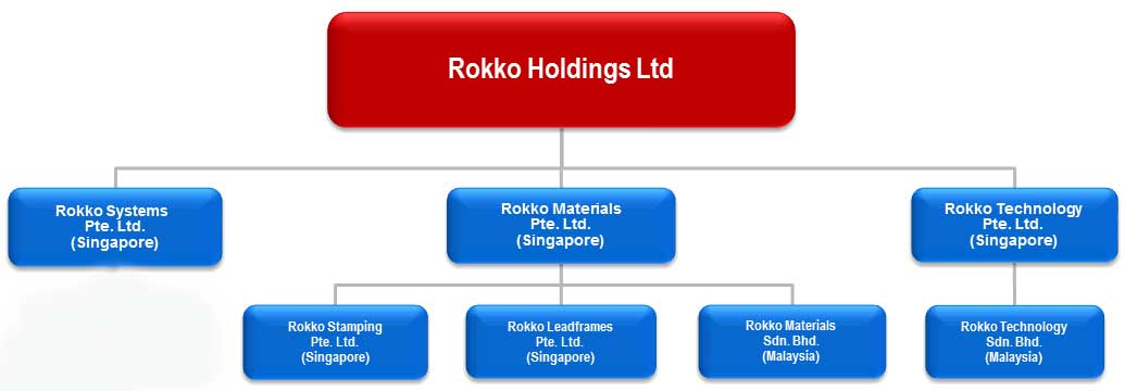
Established in 1992, Rokko is a precision engineering group principally engaged in the business of providing automated equipment and precision engineering services to customers in the semiconductor and electronics industries. The Group has 3 major business segments – Auto Vision & Robotics, Advanced Materials & Electrochemistry, and Precision Engineering.
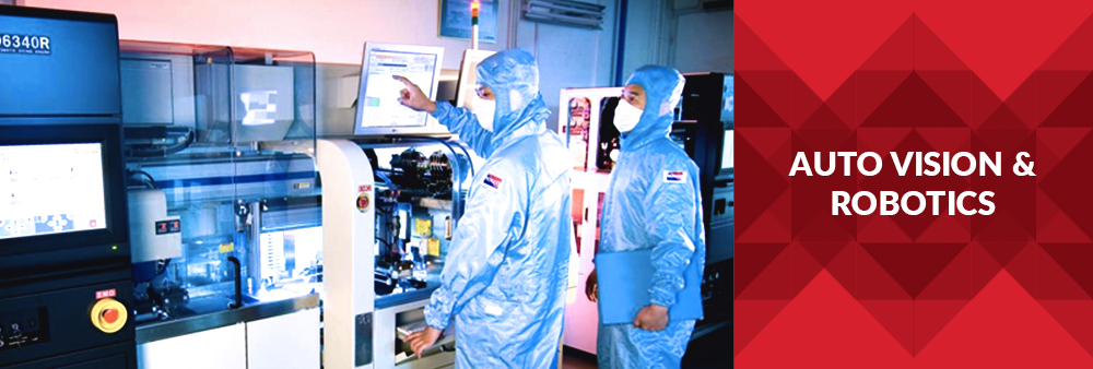
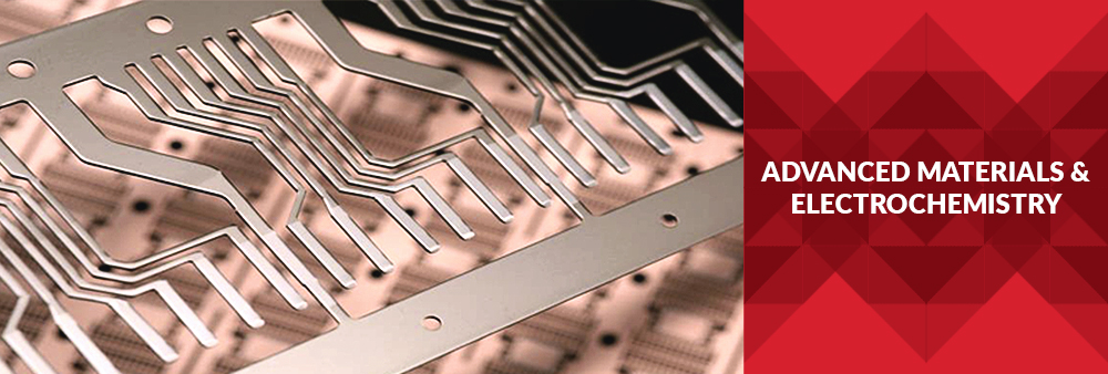
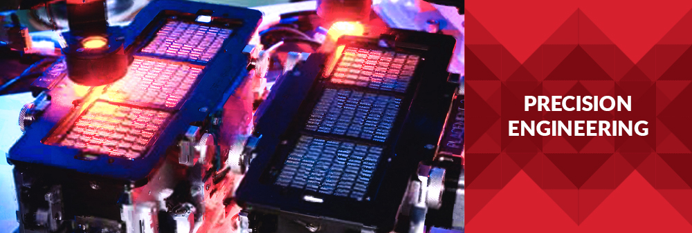
The Auto Vision & Robotics segment designs, develops and manufactures customised automated equipment specific to customer requirements under the proprietary “Rokko” brand. The Advanced Materials & Electrochemistry segment manufactures lead frames for the semiconductor industry as well as provides precision connector stamping and plating services to manufacturers in the electronics industry. The Precision Engineering segment designs, develops and manufactures precision engineering used in the front and back-end semiconductor manufacturing processes.
Our customer base spans across Southeast Asia to North Asia and certain parts of Europe. The group has manufacturing facilities in Singapore and Malaysia and an established presence in Indonesia, Taiwan, The Philippines and China.

Our dedicated team specialises in design, development and manufacturing of automated equipment for our customers use in the semiconductor “back-end” assembly processes. The equipment is customised to meet our customers requirements and is marketed under our proprietary “Rokko” brand- Auto Vision and Robotics.
material-div

With our in-house precision engineering capabilities, we provide high speed connectors to major manufacturers in the electronics industry. Our precision stamping for various types of connectors are mainly used in disc drives, which connect electronic products to devices that transmit electronic signals. We possess core capabilities in metal stamping, chemical etching and electroplating for a wide range of semiconductor leadframes for back-end semiconductor manufacturers.
precision-div

We design, develop and manufacture precision tools and dies for use in the front-end and back-end processes in the semiconductor chips assembly. The “front-end” assembly process involves die bonding and wire bonding processes whereas the “back-end” process involves the mold packaging, singulation and the final testing of fully assembled semiconductor chips.

Have a question?

Call our staff OR drop us an email

Comments are closed.